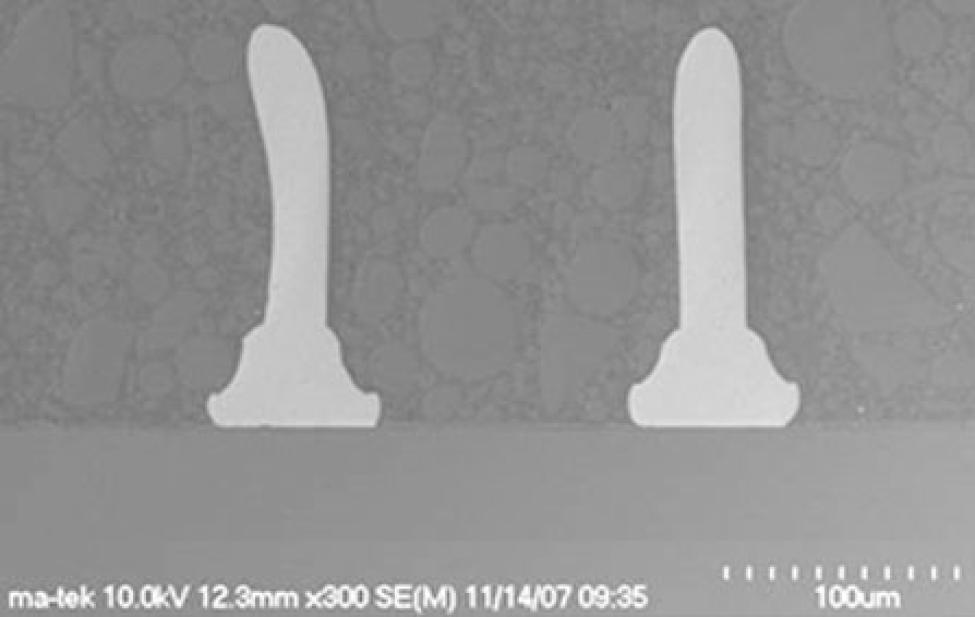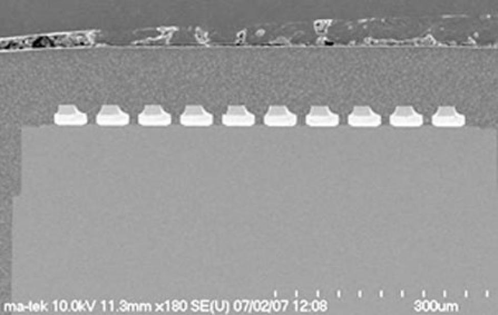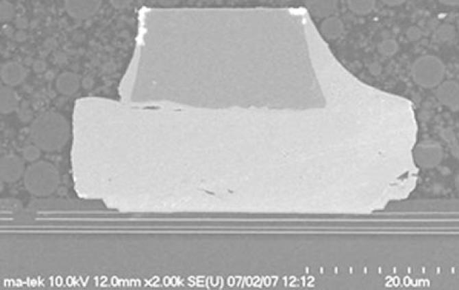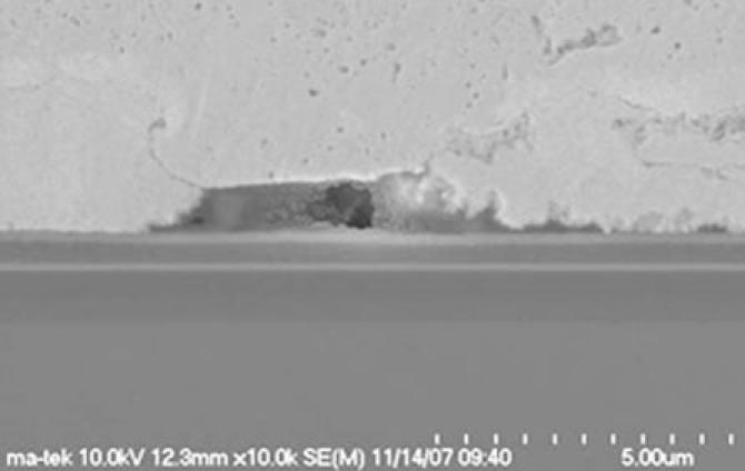
Package Structure
封装结构与外观分析
封装结构与外观是判断制程品质的第一道关卡。透过外观、尺寸与结构量测,可及早发现封装变形、翘曲或结构异常,避免问题进一步扩大。
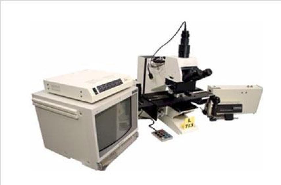
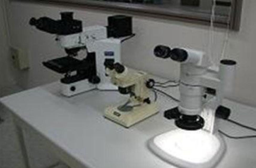
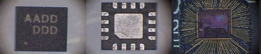
Optical Microscope
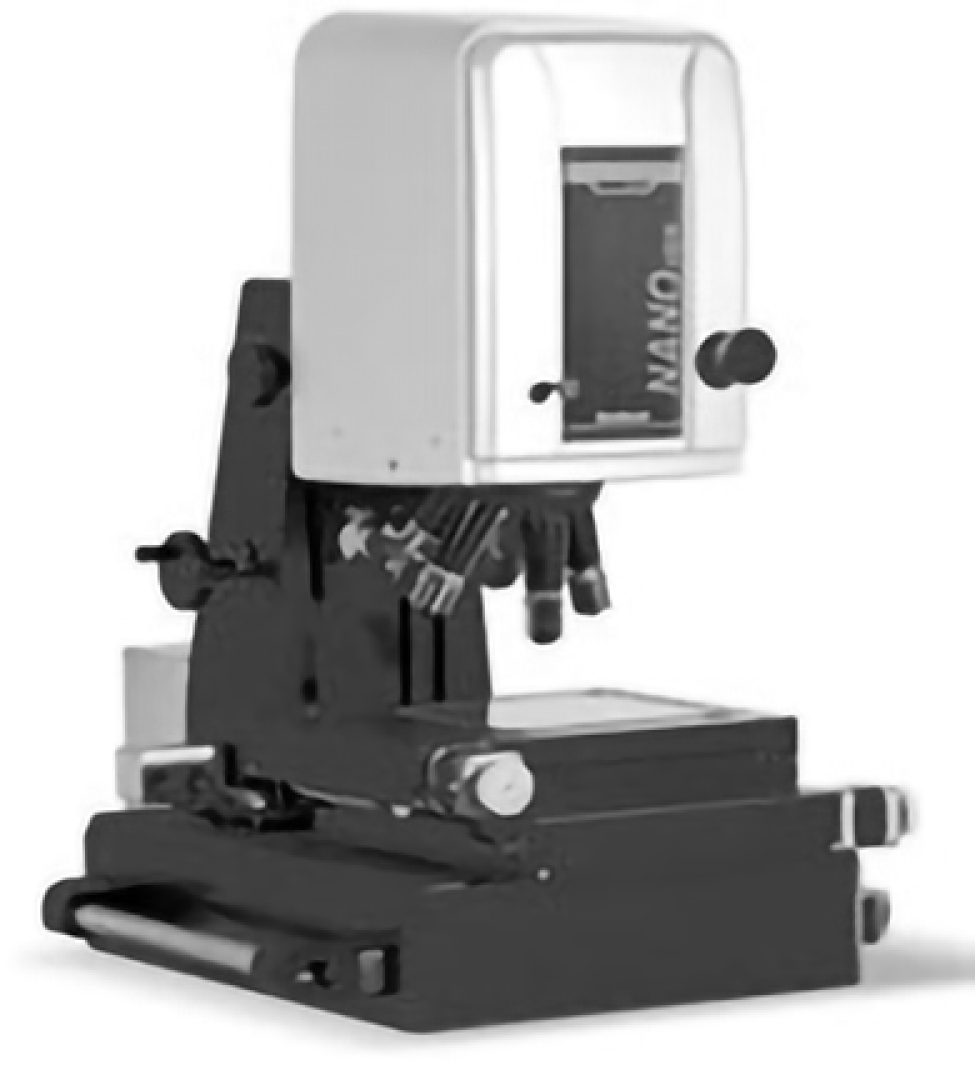
Non Contact 3D Surface Profiler
Applications
- Flatness, surface roughness, step height, deformation and waviness
- 2-D and 3-D profile
Advantages
- Accurate, fast and no sample preparation is needed
- An extremely wide range of surface heights is capable to be profiled. (~180μm)
- The benefits of optical surface profilometry include
- Excellent height resolution
- High measurement speed
- Ability to perform non-contact measurements of delicate surfaces
Surface defects characterization
-
-
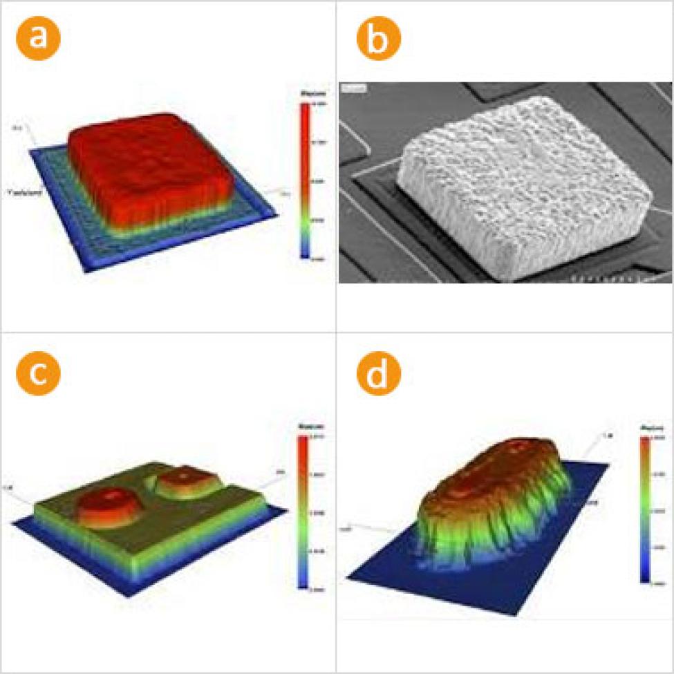
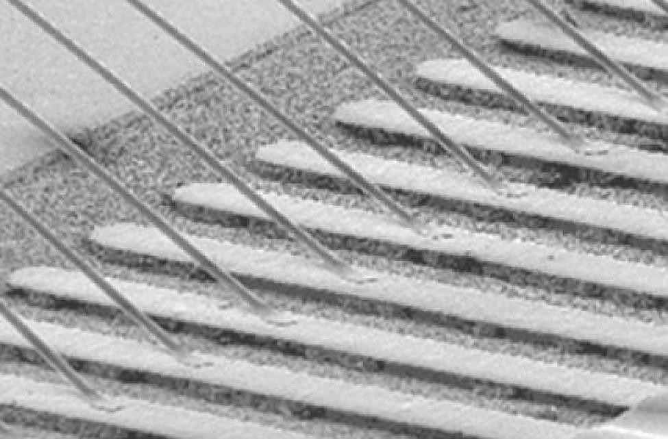
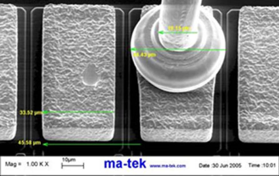
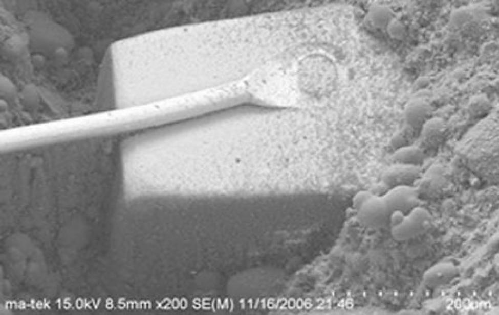
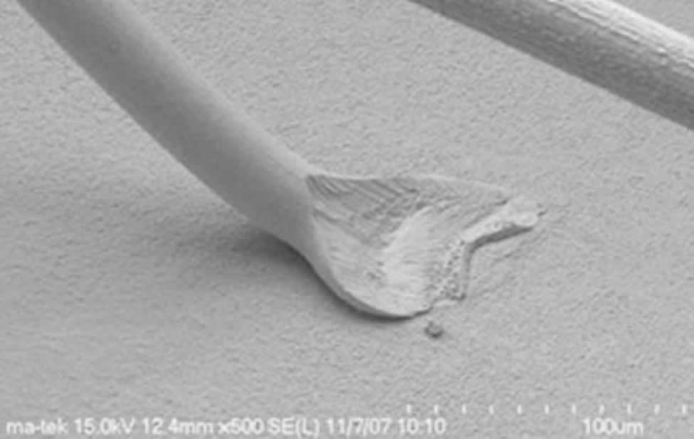
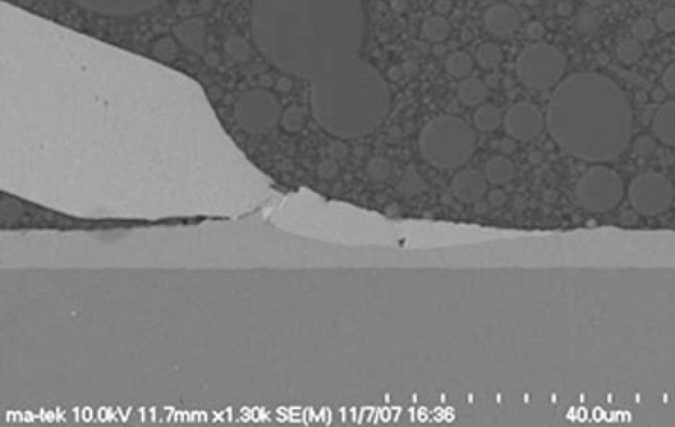
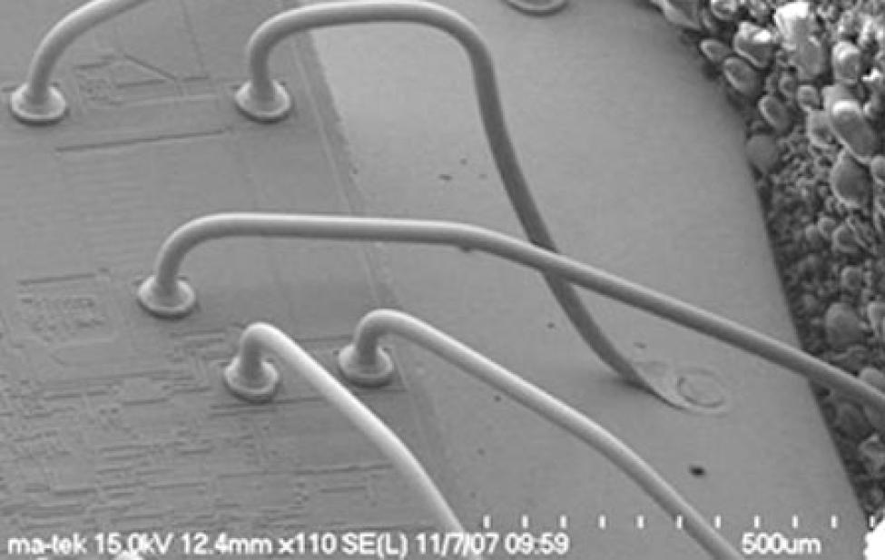
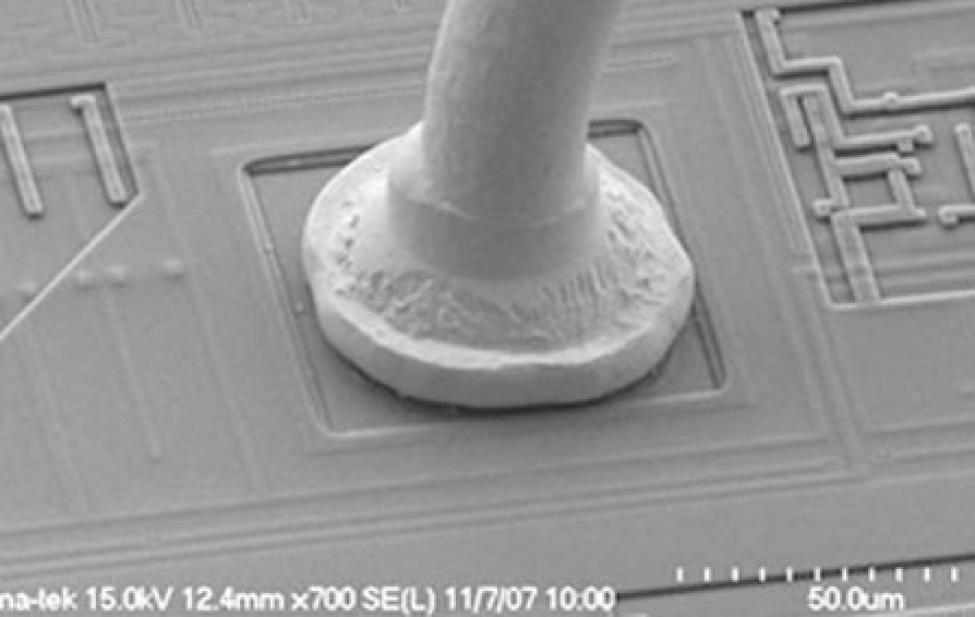
(a) OP;(b) SEM;(c) LED ;(d) Au Bump
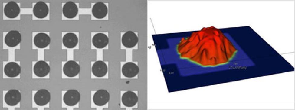
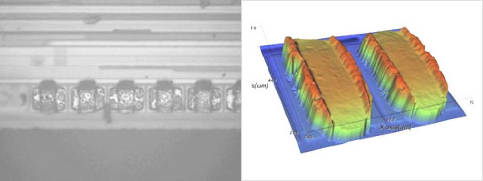
-
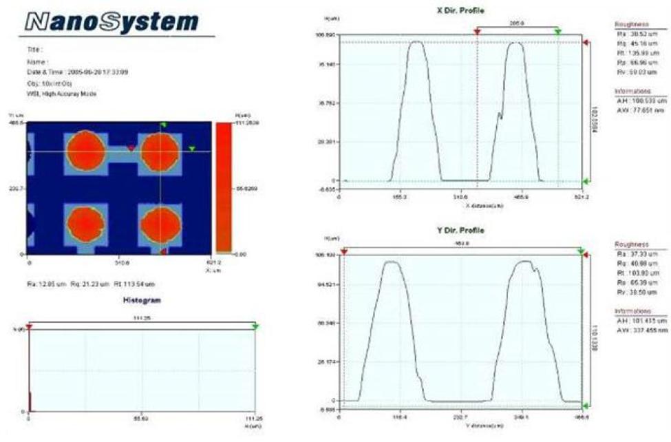
100 μm Bump Profiler
-
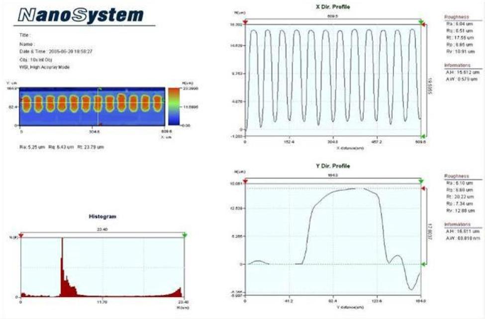
20 μm Bump Profile
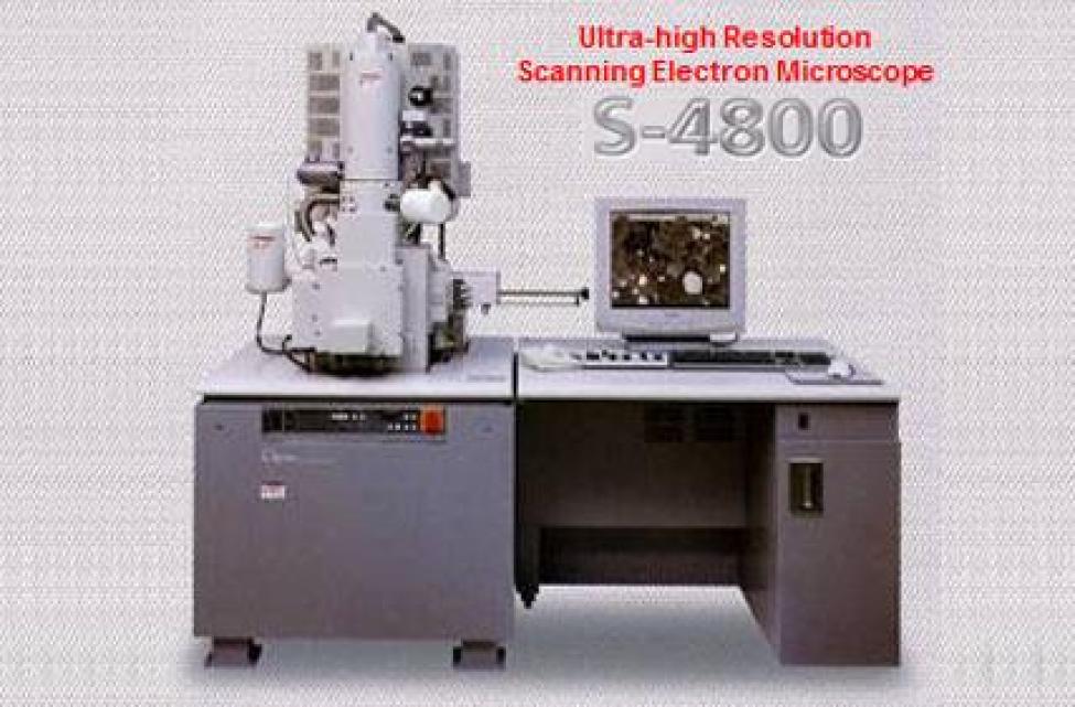
SEM Imaging